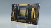
Nvidia unveiled its A100 artificial intelligence chip, which houses 54 billion transistors and can execute 5 petaflops of performance, about 20 times more than the company’s previous Volta chip. Chief executive Jensen Huang, who revealed it during his Nvidia GTC keynote address, dubbed it “the ultimate instrument for advancing AI.” The original March 24 introduction was postponed due to the COVID-19 pandemic. Nvidia also unveiled the DGX A100 system, the third generation of Nvidia’s AI DGX platform, which uses the new chips. The DGX A100 is now shipping.
VentureBeat reports that, “the U.S. Department of Energy (DOE) Argonne National Laboratory will first get the chips, which it will use “to better understand and fight COVID-19.” According to Rick Stevens, associate laboratory director for computing, environment and life sciences, “the DGX A100 system’s power will enable scientists to do a year’s worth of work in months or days.”

The Nvidia DGX A100 systems, which start at $199,000, are shipping through the company’s Partner Network resellers around the world.
Nvidia director of product management datacenter and cloud platforms Paresh Kharya said, “the 7-nanometer chip, codenamed Ampere, can take the place of a lot of AI systems being used today.” To put it in context, AI training today requires 600 CPUs at a cost of $11 million, 25 racks of servers and 630 kilowatts of power.
Nvidia said that Ampere “can do the same amount of processing for $1 million, a single server rack, and 28 kilowatts of power.”
In addition to the new chipset, the DGX A100 system uses “eight of the new Nvidia A100 Tensor Core GPUs, providing 320 gigabytes of memory for training the largest AI data sets, and the latest high-speed Nvidia Mellanox HDR 200Gbps interconnects.”
Nvidia also introduced its “next-generation DGX SuperPOD, a cluster of 140 DGX A100 systems capable of achieving 700 petaflops of AI computing power.” Nvidia built its own DGX SuperPOD by “combining 140 DGX A100 systems with Nvidia Mellanox HDR 200Gbps InfiniBand interconnects” and intends to use it “for internal research in areas such as conversational AI, genomics, and autonomous driving.”
Kharya said it took the company three weeks to build and that it is “one of the world’s fastest AI supercomputers — achieving a level of performance that previously required thousands of servers.” Nvidia released “DGX SuperPOD reference architecture … to help its customers build their own A100-powered datacenters.” The blueprint “follows the same design principles and best practices Nvidia used.”
The Nvidia A100 chip uses the same Ampere architecture … that could be used in consumer applications such as Nvidia’s GeForce graphics chips.” Unlike Advanced Micro Devices (AMD), VB says, “Nvidia is focused on creating a single microarchitecture for its GPUs for both commercial AI and consumer graphics use.” But Nvidia would “configure an Ampere-based chip in a very different way” for computer graphics.
The Verge says that, “the A100 uses high-bandwidth memory for datacenter applications, but that wouldn’t be used in consumer graphics … [and] the cores would also be heavily biased for graphics instead of the double-precision floating point calculations data centers need.”
Nvidia has posted a series of videos related to the GTC 2020 event.

No Comments Yet
You can be the first to comment!
Sorry, comments for this entry are closed at this time.